

Introduction
So you are a software engineer looking to branch into hardware. Or maybe you already design circuit boards and want to know what tools are best in 2026. Either way, picking the right PCB software design platform can feel overwhelming.

The market is growing fast, and new options appear all the time.
The global PCB design software market is exploding. One report shows it was worth about USD 4.13 billion in 2025 and is predicted to hit USD 16.02 billion by 2035, growing at a steady 14.52% each year. That growth comes from more complex electronics, more IoT devices, and smarter tools like AI and cloud collaboration. The PCB design software market size is clearly on the rise.
For software engineers, this is great news. Hardware design is becoming more accessible than ever. Many software design PCB tools now feel familiar, with scripting, automation, and version control built in. But with so many choices, how do you pick the right one?
That is where this guide comes in. We will walk you through the top PCB design software options in 2026, the key features to look for, and how to decide based on your project and skill level. Whether you are designing simple two-layer boards or complex multi-layer circuits, you will find practical advice here.
AI is a major force driving these tools forward. Modern PCB software design platforms now include smart routing, error checking, and even auto-placement powered by machine learning. To stay on top of these fast-changing AI trends, consider subscribing to The AI Newsletter Worth Reading for clear daily updates on AI in tech and engineering.
Let us start with the basics of what makes a great PCB design tool in 2026.
What Is PCB Software Design and Why Should Software Engineers Care?
PCB software design simply means using computer-aided design (CAD) tools to lay out a printed circuit board. Engineers also call these electronic design automation (EDA) tools. They let you place components, draw copper traces between them, simulate how the board will behave, and generate the files needed to manufacture it.
For a long time, only electrical engineers touched PCB design. But 2026 is different.

The line between software and hardware work has blurred. More software engineers now work on IoT sensors, custom AI accelerators, embedded systems, and robotics. Every one of those projects needs a circuit board at its heart.
Here is the thing. Today’s PCB design software platforms look and feel a lot like the dev tools you already use. They support scripting in Python or Tcl. They play nice with version control systems like Git. Many include simulation environments so you can test your design before sending it off to a fab house. Some even hook into modern CI/CD pipelines, giving your hardware layouts the same automated checks your code gets.
Why should you care? Three big reasons.
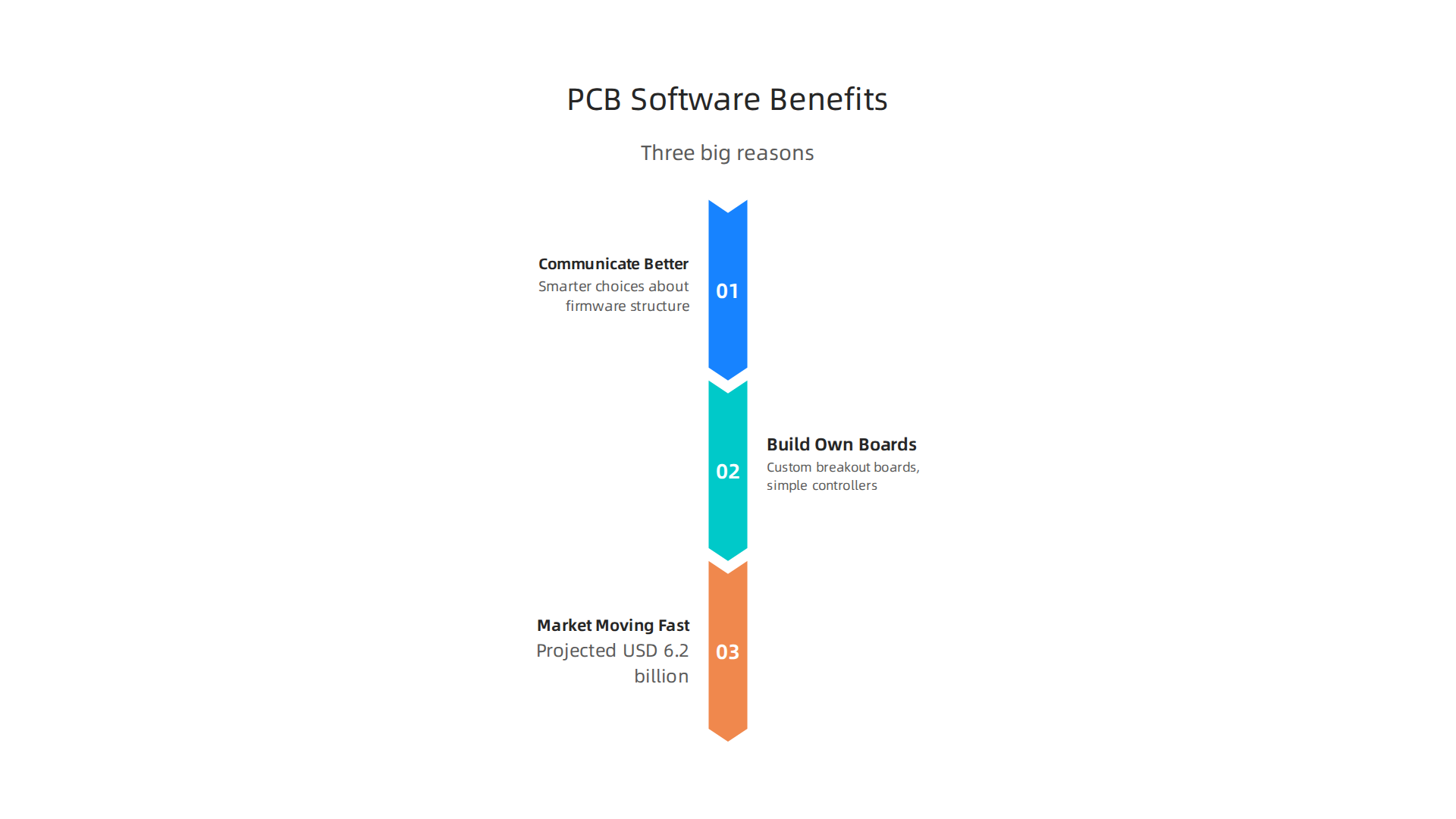
First, understanding software design PCB tools helps you communicate better with hardware teams. When you know how a board is laid out and what limits the hardware engineers face, you make smarter choices about firmware structure, pin assignments, and signal routing.
Second, you can build your own boards. Imagine whipping up a custom breakout board for a sensor you want to test, or designing a simple controller for a weekend project. With modern tools, the learning curve is way shorter than it used to be.
Third, the market is moving fast. One study shows the PCB Design Software Market growth forecast projecting the industry to hit USD 6.2 billion by the end of 2026, with a growth rate over 15% each year through 2036. More people are jumping into board design than ever before.
If you are a software engineer wondering whether to dip into hardware, the answer is yes. The tools are ready, the need is real, and your existing skills transfer well. To see how these changes fit into the bigger picture of what is happening in tech work, read this breakdown of engineering technology trends 2026.
Now let us talk about the features you should look for when picking your first PCB design tool.
Key Capabilities to Look for in PCB Design Software
When you start shopping for your first pcb design software, the choices can feel overwhelming. But most tools share a common set of features. If you know what to look for, picking the right one gets much easier.
Start with the core capabilities that every tool needs.
First is schematic capture — this is where you draw the electronic circuit using symbols for each component. Next comes PCB layout, where you place those components on a virtual board and draw copper traces to connect them. A good tool also includes routing tools that help you lay those traces cleanly, plus 3D visualization so you can see how the finished board will look inside its enclosure. These four pieces form the foundation of any solid software design pcb workflow.
Once you master the basics, look for advanced features that save time and catch errors. Design rule checking (DRC) automatically flags mistakes like traces that are too close together. SPICE simulation lets you test how your circuit behaves before you build it. For high-speed designs, signal integrity tools help you avoid signal loss. Many modern tools also include auto-routing, which handles simple trace routing for you. As one 2026 comparison of tools notes, these advanced features like AI-assisted routing and built-in SPICE simulation are now time multipliers, not just nice extras. You can see what that looks like in this top PCB design software comparison for 2026.
Collaboration features have become just as important, especially for remote teams. The best pcb software design platforms now offer cloud storage, real-time co-editing, and version control integration similar to Git. This means your hardware layout gets the same collaborative workflow your code does. Tools that support browser-based editing let teammates review and comment without installing heavy desktop software.
If you are excited about how AI is starting to help with automated placement and routing, you might also want to stay current on broader AI trends in software. The AI Newsletter Worth Reading delivers clear daily updates that keep you ahead of the curve.
Building hardware skills alongside your software expertise is a smart move. For a broader look at what skills matter most this year, check out this guide to software developer skills for 2026.
Schematic Capture and Simulation
Before you place a single component on a board, you need a clear picture of how everything connects. That is where schematic capture comes in. Think of it as the blueprint stage of your pcb software design process.
Modern tools turn this step into a real productivity booster. Instead of drawing every resistor and capacitor from scratch, you can now pull from shared component databases and reuse entire circuit blocks. This cuts down on repetitive work and ensures your parts are accurate from the start. Library governance and part intelligence are now core features that separate great tools from average ones, as highlighted in this detailed PCB design software features breakdown.
Once the schematic is ready, the real magic happens in simulation. Tools like SPICE and IBIS let you test how your circuit behaves without actually building it. You can catch signal problems early and avoid costly re-spins on your software design pcb project. This shift from "build then test" to "simulate then build" is one of the biggest time savers for hardware engineers today.
A growing differentiator in 2026 is scripting support. Tools that let you automate simulation runs with Python give you a serious edge. You can run hundreds of scenarios overnight and wake up to a fully validated design.
If you find yourself wondering how these hardware development trends fit into the bigger picture of engineering, exploring broader engineering technology trends 2026 can give you valuable context.
Layout, Routing, and 3D Visualization
After your schematic is ready and simulated, the next step is bringing it to life on the board. This is where layout tools take over in your pcb software design workflow.
First comes component placement. You decide where each part sits on the board. A good layout tool helps you group related parts and manage layer stackup. From there, you move to routing. This means drawing the copper traces that connect everything. Advanced routing features like differential pairs and length tuning help you handle high-speed signals without errors. Many tools now offer both interactive and auto-routing, letting you choose based on complexity. In fact, modern pcb design software has shifted from just drawing traces to being a full manufacturing-aware system, as noted in this PCB design software comparison for 2026.
Once traces are placed, 3D visualization lets you inspect the board from every angle. You can spot mechanical conflicts, check clearances, and export models for your mechanical team through CAD integration. This saves you from costly mistakes before you ever send the board to fabrication.
As you build these skills, thinking about overall team productivity becomes just as important. The developer experience roadmap for 2026 offers practical ways to improve your engineering workflows.
And if you want to keep up with fast-changing tech trends like AI-assisted routing, get clear daily AI updates from The AI Newsletter Worth Reading.
Top PCB Design Software Tools in 2026: An Overview
Once you understand the layout and routing process, the next big question is which tool to use. The pcb software design market in 2026 offers solid options for every skill level and budget. Here is a breakdown of the main categories.
Traditional Leaders Still Dominate the High End
If you work in a professional environment with complex multi-layer boards, Altium Designer, Cadence Allegro, and Siemens PADS (formerly Mentor PADS) remain the top choices. These tools come with powerful simulation, advanced routing, and tight manufacturing integration. They also cost more. For a direct feature and price comparison, check out this Altium Designer vs OrCAD comparison to see how the full-featured suites stack up.
Cloud-Native Tools Are Gaining Ground
Browser-based platforms like EasyEDA, CircuitMaker, and Upverter are becoming popular with hobbyists, students, and distributed teams. You do not need to install heavy software. Everything runs online, and your designs live in the cloud. This makes collaboration and version control much simpler. The complete PCB design software list 2026 includes these options with notes on pricing and features.
Open-Source Has Come a Long Way
KiCad used to be a beginner-only tool. Not anymore. In 2026, KiCad and LibrePCB have matured so much that many companies now use them for real commercial projects. The software is free, the community is active, and you get professional features like hierarchical schematics, 3D viewer, and design rule checking. This ranking of EDA tools for PCB design 2026 places KiCad as the open-source leader with advanced capabilities.
Which One Should You Choose?
Your choice depends on your project size, budget, and team setup. For serious professional work, go with the traditional platforms. For fast collaboration, try cloud-native. And if you want powerful features without the price tag, open-source is ready for you. As you evaluate these tools, thinking about overall developer productivity can help. This guide on engineering technology trends in 2026 shows how AI and platform engineering are changing the way teams build hardware and software together.
Take the time to test a few options. The right pcb design software will save you hours on every board you build.
Traditional Industry Leaders
Now let us look closer at the heavy hitters you will find in most professional engineering departments. These platforms power everything from consumer gadgets to aerospace systems.
Altium Designer remains a top choice for many teams.
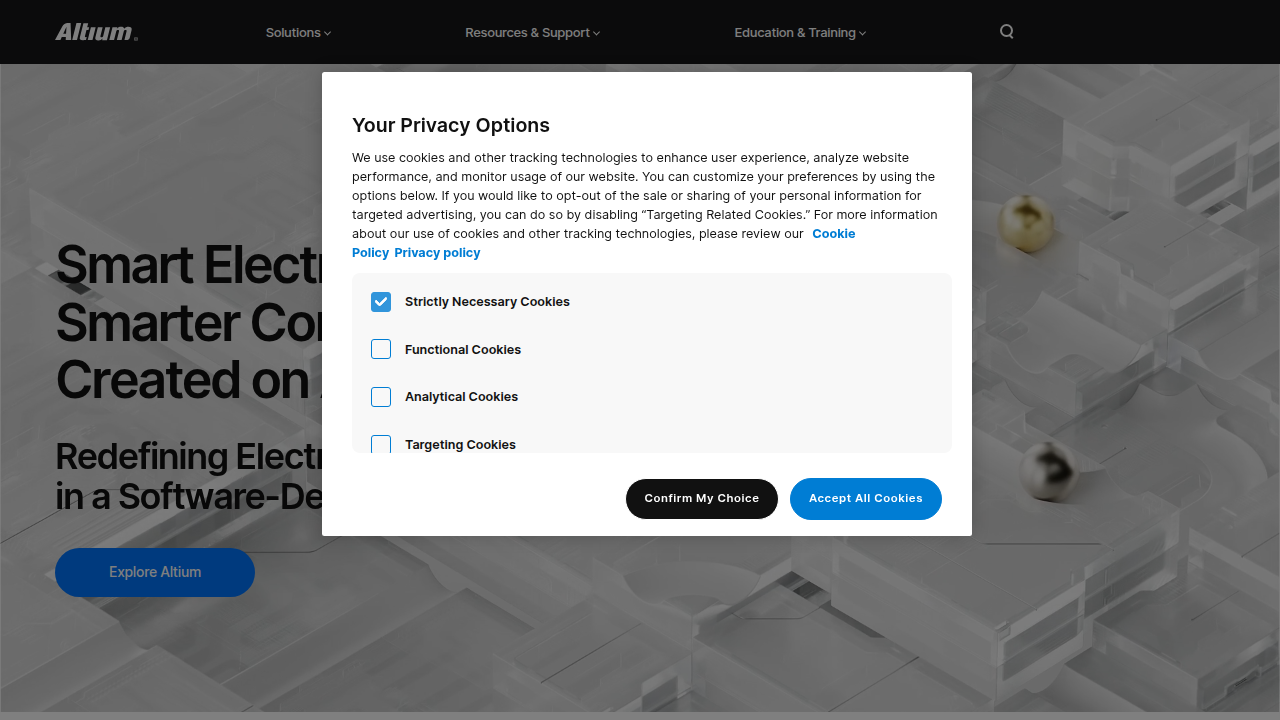
It brings schematic capture, PCB layout, advanced routing, and component management into one unified environment. This saves time because you do not need to jump between separate programs. The library tools let you manage thousands of parts with ease. For a detailed look at how it compares to other platforms, see this Best PCB Design Software comparison.
Cadence Allegro and OrCAD are the go-to options for high-speed, complex designs.

Companies in aerospace and telecom rely on them because they handle strict signal integrity requirements and dense multi-layer boards. The learning curve is steeper, but the control is unmatched for serious projects where precision matters most.
Mentor PADS (now Siemens PADS) sits between the high end and mid-range. It gives you professional power without the top-tier price. Many small to medium businesses use it as their daily driver for reliable, production-ready boards.
As these tools evolve, they keep adding AI-powered routing and automation. Staying on top of these changes can save you hours on every build. Many engineers now rely on a trusted source for daily updates. You can subscribe to the The AI Newsletter Worth Reading for clear daily AI insights that help you stay ahead.
Also, learn how personal AI assistants reshaping developer workflows can make your design process even smoother.
Emerging and Cloud-Based Solutions
Not every team needs a heavy desktop install to get good work done. In fact, many engineers in 2026 are moving toward cloud-based tools that let them design from anywhere. Here are a few options worth knowing about.
Autodesk Fusion 360 (which now includes what used to be Eagle) is a big player here. It blends electronic design with mechanical design in one platform. That is a huge win if your team builds products where the PCB has to fit tightly inside a case. Startups love it because you can check how your board fits inside the enclosure before you ever send it to manufacturing.
EasyEDA paired with LCSC offers something totally different.
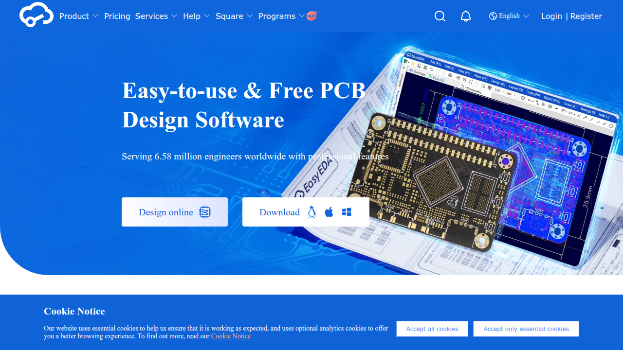
It runs right in your browser with no install needed. The best part is the direct link to component sourcing. You design your board, and with a few clicks you can order the parts from LCSC’s inventory. That makes it a great pick for hobbyists and small teams on a budget. For a broader look at what is available, check out this best PCB design software comparison in 2026.
Upverter takes a different approach. It is built for teams who want to collaborate in real time. Version control is baked right in, which means no more emailing files back and forth. Everyone sees the same live schematic.
The rise of these browser-based tools is changing how engineers think about pcb software design. You no longer need a powerful workstation to get started. A decent laptop and a browser is enough. Learn how personal AI is the productivity revolution software teams need to make the most of these modern design workflows.
How to Choose the Right PCB Design Software for Your Team
Picking the right tool for your team can feel overwhelming in 2026. There are so many options, and each one promises something different. But the decision gets easier when you focus on a few key questions.
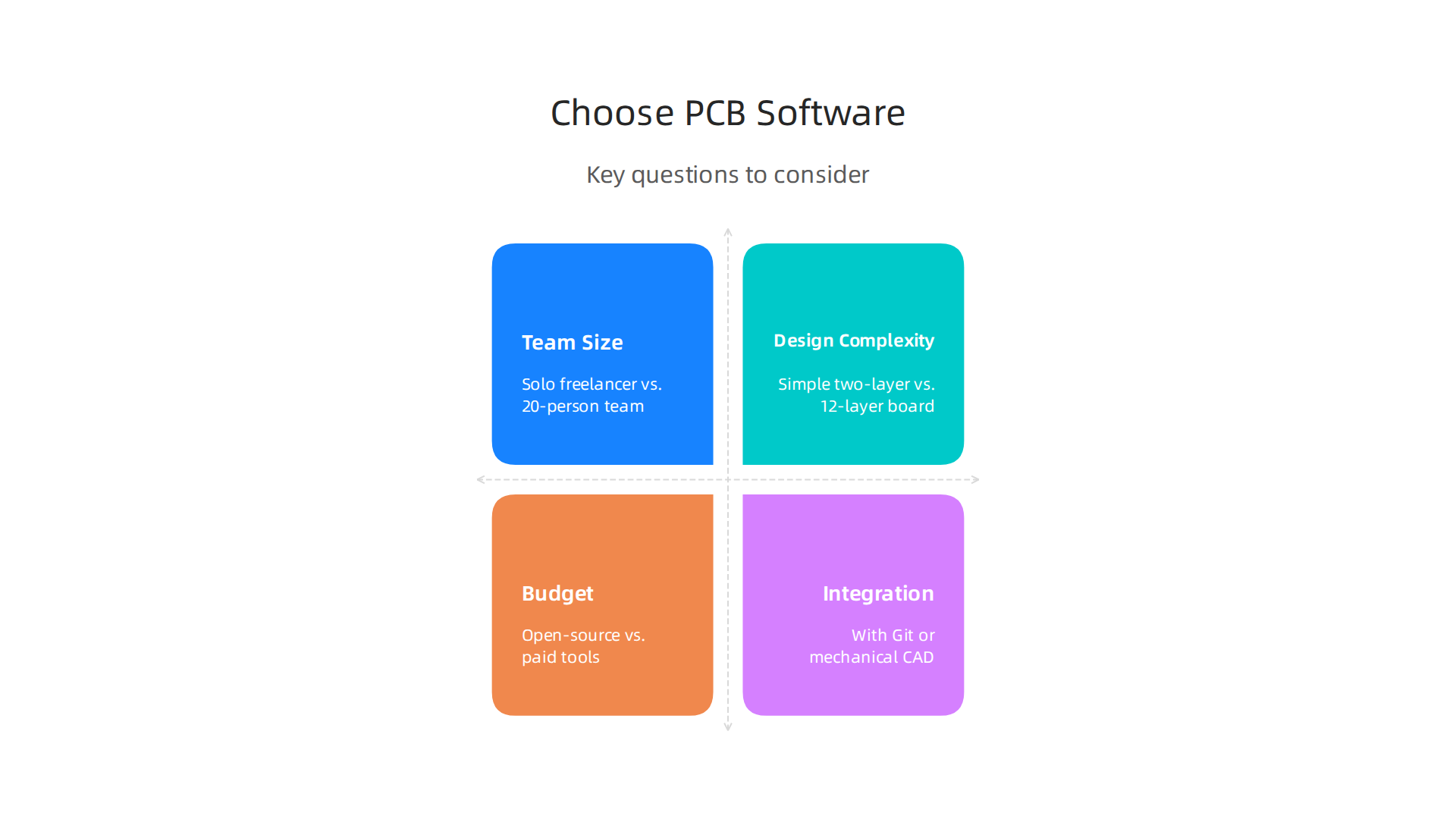
First, think about team size. A solo freelancer does not need the same features as a 20-person hardware team. Cloud-based tools like the ones we just covered work great for small teams because collaboration is built in. Larger teams might need something with more control, like Altium Designer or KiCad with a Git backend.
Design complexity matters too. Are you routing a simple two-layer board for a sensor? Or are you laying out a high-speed 12-layer board with impedance control? The more complex your designs, the more you need robust simulation and rule checking. According to the Best PCB Design Software in 2026: Tools Compared guide, AI features are now common in mid-range and premium tools, automating footprint generation and layout hints.
Budget is the next big filter. Open-source software like KiCad costs nothing upfront but has a steeper learning curve. Paid tools like Altium or Fusion 360 come with support and polish but can cost thousands per seat. Many teams start with a community edition or free trial before committing. That is a smart move.
Integration with your existing workflow is another factor. If your team already uses Git for version control, choose pcb design software that supports Git natively. KiCad 9.0 and Altium both offer good Git integration. If you work with mechanical engineers, Fusion 360 might make more sense because it blends PCB and CAD in one place.
Finally, evaluate the learning curve. Open-source tools often have less documentation and smaller communities. Paid tools usually offer tutorials and support. The best way to test is to try before you buy. Most commercial tools offer free trial versions.
Stay ahead of the curve by keeping up with the latest engineering trends. The engineering technology trends 2026 article covers how AI and platform engineering are reshaping development, including the tools you will use for software design pcb.
And if you want daily AI updates that actually help you make better tool decisions, sign up for The AI Newsletter Worth Reading. It delivers clear, practical insights straight to your inbox.
Integration with Engineering Workflows
Once you pick your tool, the next question is how well it fits into your existing workflow. In 2026, the best pcb software design tools do not live in isolation. They connect with the systems your team already uses for version control, automation, and mechanical design.
Git integration is now a must-have feature for pcb design software. Both KiCad 9.0 and Altium offer built-in support for Git. This means you can track every change to your schematics and layouts, just like you track code. The Reddit community has confirmed that Git for PCB design actually works with these tools. You commit your design, push it to a remote repository, and your whole team sees the latest version.
Beyond basic version control, many teams now set up continuous integration and continuous delivery (CI/CD) pipelines for their hardware. Every time you commit a change, the pipeline can run design rule checks, generate Gerber files, and even create a bill of materials. Resources like the guide on setting up a CI/CD pipeline for PCB designs show you exactly how to automate these tasks using GitLab runners or GitHub Actions. This automation saves hours of manual work and catches errors early.
APIs also play a big role. Modern software design pcb tools expose APIs that let you extract netlists, run design rule checks, or generate BOMs programmatically. You can plug these into your existing DevOps pipeline without clicking around in the GUI.
Finally, ECAD-MCAD collaboration is critical for teams that build physical products. When the PCB designer and the mechanical engineer work in separate tools, conflicts happen. Tools that offer live synchronization between electrical and mechanical designs reduce rework and speed up time-to-market. For teams looking to refine their overall approach, understanding context engineering for agile and devops teams can help you build smoother workflows across the entire product development lifecycle.
The more seamlessly your PCB tool connects with your engineering stack, the faster and more reliably you ship.
Cost, Licensing, and Open-Source Alternatives
Cost is often the first thing people look at when choosing pcb software design tools. But the upfront price tag does not tell the whole story. Commercial tools can range from a few hundred to tens of thousands of dollars per license each year. Altium Designer, for example, costs thousands per seat annually. Many vendors now push subscription models that bundle cloud storage and technical support. That subscription fee adds up fast across a whole team.
On the other end, open-source pcb design software like KiCad is completely free. You can download it and start using it in commercial projects without paying anything. KiCad has improved dramatically in the last few years, and many designers now rely on it for serious production work. The Reddit community often points beginners to KiCad as a great starting point What PCB design software should I use?.
But free does not mean zero total cost. You still need time to learn the tool, set up component libraries, and fix bugs when they pop up. A total cost of ownership (TCO) analysis shows that the real comparison is more complex. One article explains that the total cost of ownership of open source compared to commercial software depends heavily on your team’s support needs and how much in-house effort you can invest. Another detailed breakdown of PCB design software tools found that labor costs dominate the picture, and KiCad’s TCO can be very competitive once you account for the lack of license fees The True Cost of PCB Tools in 2026: Altium vs. KiCad vs. Quilter.
Ultimately, the right choice depends on your budget, your team’s skills, and how much you value vendor support. As you weigh your options, staying informed about broader tech trends can help you make smarter decisions. For a look at how AI and platform engineering are reshaping development costs, check out the engineering technology trends 2026 overview.
If you want to keep up with the latest in tech and AI, including tools that can cut your development costs, subscribe to The AI Newsletter Worth Reading for daily updates.
Future Trends in PCB Design Software
Now that you understand the cost landscape, let’s look at where PCB design software is heading.

The tools you choose today might look very different in just a couple of years. Here are the biggest changes coming.

AI-driven auto-routing and design optimization are becoming mainstream. Instead of spending hours manually placing traces, you can let the software find the best paths automatically. Modern pcb design software uses machine learning to learn from thousands of past layouts and suggest routing that reduces signal interference and keeps boards smaller. This cuts design time significantly and helps even junior engineers produce professional work.
Cloud-based collaboration and real-time co-design are reducing iteration times. In the past, teams would email files back and forth. Now, platforms let multiple engineers work on the same board at the same time, see changes instantly, and leave comments. This is a game changer for remote teams. It means fewer meetings and faster turnaround when you need to fix a problem. As software design pcb tools move to the cloud, version control headaches disappear too.
Integration with digital twins and simulation ecosystems will further blur the line between hardware and software design. Imagine testing your circuit board in a virtual copy of the final product before you ever order a prototype. That is already happening. Digital twins let you run thermal, mechanical, and even firmware simulations together. This catches mistakes early and saves huge amounts of money on re-spins.
To keep up with how AI is transforming every part of engineering work, including PCB layout, check out how personal AI assistants are reshaping developer workflows in 2026. Staying on top of these trends helps you pick the right pcb software design tools for the years ahead.
Summary
This guide helps software engineers choose PCB design software in 2026 by outlining the market context, essential capabilities, and practical selection criteria. It explains what PCB/EDA tools do (schematic capture, layout, routing, simulation and 3D visualization), why modern platforms now feel familiar to developers (scripting, Git, CI/CD), and which features — from DRC and SPICE to AI-assisted routing and cloud collaboration — matter most. The article breaks tools into categories (traditional high-end, cloud-native, open-source), compares tradeoffs around cost and total cost of ownership, and shows how to integrate PCB tools into engineering workflows. Readers will learn how to evaluate options based on team size, complexity, and budget, how to test candidates, and what future trends like AI and digital twins mean for hardware design productivity.